Hot-wire activated Chemical Vapor Deposition (Hot-wire CVD)

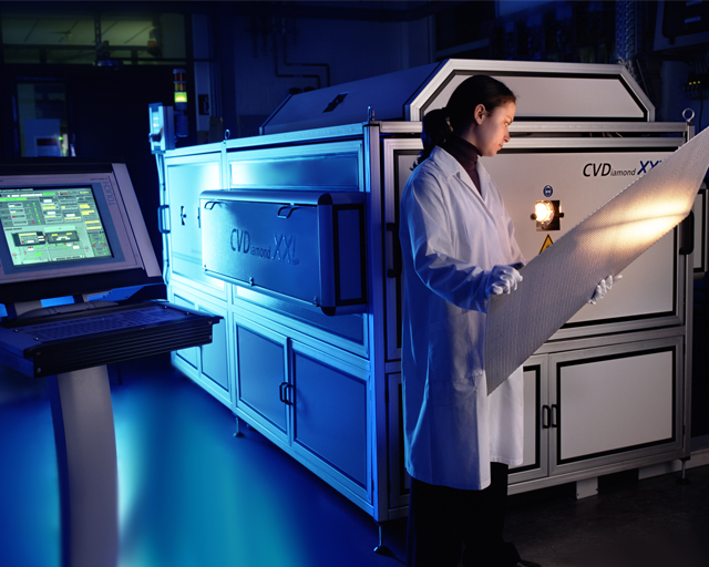
Hot-wire-activated chemical vapor deposition, short: hot-wire CVD, is a core competence of the Fraunhofer IST and permits in particular the production of crystalline diamond coatings on complex three-dimensionally shaped surfaces as well as large areas in high quality. At the Fraunhofer IST, we have at our disposal the world's largest hot-wire CVD coating plant for the production of diamond coatings on surfaces of up to 0.5 x 1 m2. This enables us to apply coatings with the highest quality and value to complex components and tools and to produce silicon-based coating systems with high efficiency and unique properties. In both cases, we develop the technologies and coating modules as well as the associated processes.
”With the largest diamond coating plant in the world and our expertise, we have the possibility of making this unique material available for your ideas.”
Dr.-Ing. Christian Stein, Group Manager
Technology and process development for the production of CVD diamond and silicon-based coating systems
The potential applications of crystalline diamond and silicon-based coating systems by means of hot-wire CVD are manifold: In addition to components and tools, they encompass optical and electronic elements, highly efficient solar cells, sensors – e. g. MEMS (micro-electro-mechanical systems) – and microsystems. CVD diamond coatings have properties comparable to natural diamond and are characterized by maximum hardness, extreme wear resistance, minimal friction coefficients and high chemical resistance. The unique material properties result in significant performance improvements and long-lasting products. Current fields of application include high-performance tools for machining and forming technology, and highly stressed parts such as mechanical seals, bearings or guide components.
Process and system expertise
We have acquired extensive expertise in the design and manufacturing of CVD diamond coatings, covering both specific treatment sequences (material selection, pretreatment, coating and process development, qualification) and the application. We provide support in the related production and process-chain considerations, in the testing and evaluation of systems, and in technology transfer all the way through to the individual design of coating systems, processes and hot-wire CVD coating technology.
Hot-wire CVD systems for diamond coating

Fully automated HFCVD systems developed at the Fraunhofer IST allow coating on surfaces of up to 1000 x 500 mm². In addition, facilities and processes are available for the diamond-coating of complex components and tools and for internal diamond coating. Possible materials for coating include hard metals, ceramics (especially SiC, Si3N4), refractory metals, silicon and glasses.
Specifications / technical data
- Large-surface coating (500 x 1000 mm2) with polycrystalline diamond coatings
- Diamond-coating of components and tools and for internal diamond coating
Hot-wire CVD inline system

Hot-wire CVD also offers decisive advantages in the production of silicon-based coatings compared to commonly used plasma-assisted coating processes:
- High gas yields
- High coating rates
- Simple system technology
- Easy to scale up to large coating areas
- High-energy particle bombardment offers gentle coating process without damage to substrate and growing layer
- High energy efficiency
- Low “Total Cost of Ownership“.
With our inline systems, areas of up to 600 x 500 mm² can be coated.